 Help Desk +1-778 878-1690
")
3D Optical Profilometer- LSPM-441
$0.00
The POINTVALUES SP-TD3200 3D Surface Profilometer is a high-precision, non-contact surface measurement system based on white light interference technology. Designed for sub-nanometer accuracy, it captures 3D morphological data with advanced Z-axis scanning and 3D reconstruction algorithms. Ideal for semiconductor, MEMS, optics, aerospace, and research applications, it evaluates over 300 surface parameters—including roughness, flatness, and micro-contours—according to ISO, ASME, EUR, and GBT standards. Featuring automated measurement, powerful noise filtering, and real-time environmental vibration detection, it ensures exceptional accuracy and repeatability.
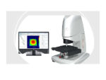
POINTVALUES 3D Surface Profilometer: SP-TD3200
POINTVALUES 3D Surface Profilometer, SP-TD3200 is a surface properties detection instrument used for sub-nanometer level measurement.
The system uses white light interference technology, combined with a precision Z-direction scanning module and 3D modeling algorithms, to conduct non-contact scanning and record 3D images of various solid surfaces.
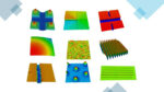
The system software processes and analyzes these 3D images, obtaining 2D and 3D parameters that reflect the surface quality, with precise 3D morphological patterns.
Applications
POINTVALUES SP-TD3200 is broadly used in semiconductor manufacturing and packaging process testing, 3D electronic glass screens and their accessories, optical processing, micro/nano materials and devices, and MEMS systems.
It is also utilized in aerospace, the defense industry, research institutes, and other fields.
It can measure the surfaces of various objects, ranging from ultra-smooth to rough, across a wide range of reflectivity.
Detectable Parameters
This system evaluates roughness, flatness, micro-geometric contours, curvature, and other metrics of workpieces at nanometer to micrometer scales.
The profilometer provides more than 300 2D and 3D parameters as evaluation criteria based on the four major domestic and international standards: ISO, ASME, EUR, and GBT.
Product Features
- Assesses various surface characteristics and microstructures by recording key metrics, including stepwise height, angle, and contour dimensions, with ±0.5% and 0.1% repeatability.
- Offers automated auxiliary functions such as autofocus, automatic stripe navigation, and automatic brightness adjustment during measurement.
- Supports automatic splicing measurement and automatic multi-area positioning measurement and analysis.
- Provides data processing with four major modules: leveling, image retouching, denoising and filtering, and region extraction.
- Facilitates analysis with one-click and multi-file analysis systems.
Data analysis includes five major functions: roughness analysis, geometric contour analysis, structural analysis, frequency analysis, and functional analysis.
Application Fields
Characterization of surface morphology and topography by precise detection of flatness, roughness, waviness, surface contour, surface defects, wear, corrosion, pores, gaps, step height, bending, and deformation, in various domains.
Performance Features
- The system combines optical interference technology, a precision Z-direction scanning module, and an advanced 3D reconstruction algorithm to ensure high accuracy.
- Noise-removal function isolates vibrations above 2 Hz, eliminating ground vibration and airwave noise, ensuring extremely high accuracy and repeatability.
- The environmental noise detection module (0.1 nm resolution) quantitatively evaluates vibration interference and supports equipment debugging, monitoring, and troubleshooting.
- A joystick with integrated displacement adjustment (X, Y, Z) enables rapid pre-measurement tasks such as stage adjustment, Z-direction focusing, and stripe navigation.
- Collision protection: ZSTOP sensors detect lens-sample contact, triggering an emergency stop to prevent damage.
- The system can connect to a stable gas source or standard air compressor and can work without an external gas source.
Remarks
- Measured Sa of 0.2 nm silicon chip in laboratory environment using EPSI mode, single stripe, full field of view 80 μm filtering.
- Roughness parameters obtained by measuring RMS of a 0.2 nm silicon chip according to ISO 25178.
- Step height parameters obtained by measuring a 4.7 µm step height standard block in compliance with ISO 10610-1:2009.
- When software noise evaluation is 4 nm ≤ 3σ ≤ 10 nm, repeatability reduces to 0.015 nm, step height accuracy to 0.7%, and step height repeatability to 0.12%.
- When 3σ > 10 nm and the environment does not meet equipment requirements, the site must be changed.
RELATED PRODUCTS
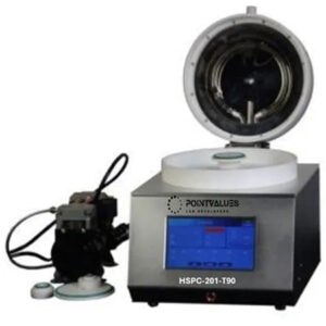
Heated Spin Coater- HSPC-201-T90
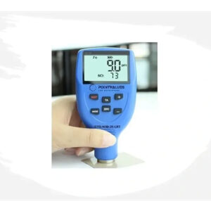
Magnetic Coating Thickness Range &#...

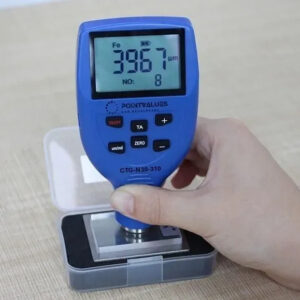
Surface Roughness Tester with Print...
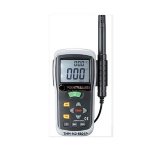
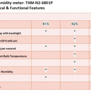
Temperature and Humidity meter- THM...
Reviews
There are no reviews yet.